TM 5-6675-320-14
ad.
Memory control logic.
The 15-bit memory address register consists of two 8-
bit bistable latches, U52 and U53, which latch the address off the plotter bus on
the rising edge of STM.
The first 13 outputs are supplied to the 8k ROMs to select
specific memory locations.
The ROMs are enabled by addresses 13 and 14 along with
STM, READ, and R10 + RAL.
The RAM address locations are accessed by the first
10 outputs of the address register.
The devices are enabled by addresses 10 and 14
along with XSMC.
The READ line determines if a READ or WRITE function is occurring.
a e . M a i n P C A A 2 i n t e r p o l a t o r c i r c u i t r y .
T h e i n t e r p o l a t o r c i r c u i t r y o f t h e m a in
PCA receives the X- and Y-velocity data from the processor, integrates, and converts
t h e d a t a i n t o a n a l o g s i g n a l s f o r t h e m o t o r d r i v e r c i r c u i t s.
During the 1024 microsecond operating cycle, the motor position is updated eight
times.
This is accomplished by adding 1/8 of the input velocity word, which is an
8-bit, signed two’s complement, with a maximum value of plus or minus decimal 90, to
the position accumulator during each of the eight subcycles. The velocity word
is added in these small increments to provide a smoother motor operation.
a f .
Operating cycle.
The interpolator operating cycle is begun with the positive
transition of the interrupt request (IRQ) from U22.
The microprocessor responds and
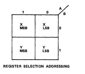
the interpolator write (W26) latches the first half of the velocity word (bus 12-15)
into one of four registers of the input data register U25 as selected by the address
b i t s ( b u s 0 - 1 ).
o f t he
places
o f t he
(1) The latching of data into U25 is accomplished during the Y-axis portion
e i g h t h s u b c y c l e o f t h e p r e v i o u s i n t e r p o l a t o r c y c l e . T h e f i r s t s u b c y c le
t h e f o u r l e a s t s i g n i f i c a n t b i t s ( L S B ) o f t h e X - a x i s i n s t r u c t i o n o n t h e i n p u t s
data selector U26.
The data selector couples the X LSB to the Y inputs of
the adder U24.
A t t h i s t i m e,
the Z inputs are the four LSBs from the previous
subcycle, input through U21.
The output of U24 is the sum of the Y and Z inputs and
the carry input (X) from the carry adder U27.
If a carry-out from the previous
summation in U24 exists, it is clocked through U27 and becomes a carry-in to U24 for
the present subcycle.
The carry input to U24 is set low every 16 clock pulses to
assure that the carry is clear at the beginning of each new cycle.
4-130