TM 5-6675-323-14
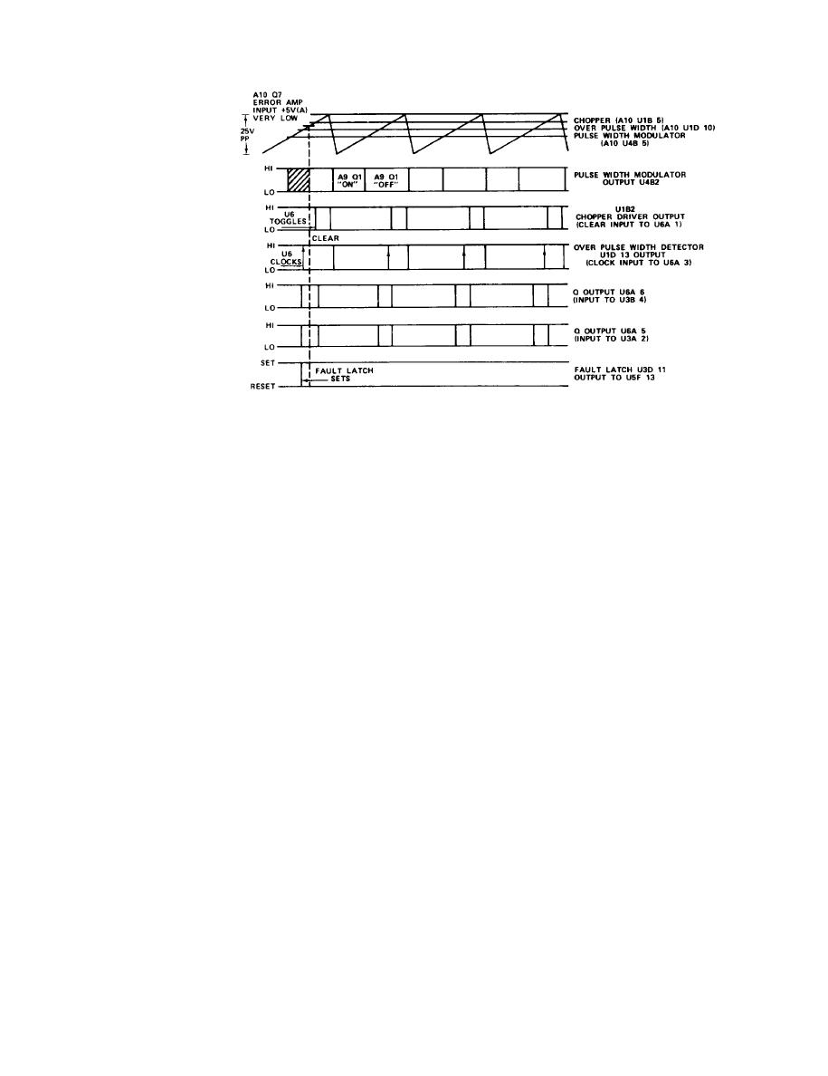
(a) When power is first applied to the plotter, transistor A10-Q5 in
the turn-on/off sequence circuit is turned on, which provides a discharge path for
any residual charge on C14 and forward biases transistor A10-Q10. Conduction of
transistor A1-Q10 ties the output of error amplifier U7 to common and disables the
p u l s e w i d t h m o d u l a t o r A 1 0 - U 4 B . A s filter capacitor A9-C24 reaches a level which can
allow proper operation of the rest of the power supply circuits, transistor A10-Q5
is turned off (by conduction of A10-Q1 and Q2) allowing capacitor A10-C14 to charge.
As transistor A10-Q10 is turning off, the resultant exponential voltage rise forces
the pulse width modulator to output (at start) small pulse widths. These pulse
widths sequentially increase in width until the normal operating pulse width is
reached.
(6) Turn-on/off sequence circuit.
In conjunction with the fault latch and
slow turn-on/off sequence circuitry, provides an orderly sequence to enable or
disable the series switch transistor A9-Q1 and controls the charge or discharge of
various circuits when the plotter is switched on or off. The turn-on/off sequence
circuit is immune to at least 1-1/2 missing cycles and will continue to operate with
power outages of less than 30 msec duration.
(a) Turn-on is initiated when power is first applied to the plotter,
c a p a c i t o r A9-C24 starts to charge and transistors A10-Q2, Q3, Q4, and Q5 start to
t u r n o n . V o l t a g e comparator A10-U1C acts as a voltage comparator with hysteresis to
p r e v e n t the power supply from shutting down during a momentary dropout of the main
ac source and plotter.
(b) Conduction of transistor Q4 resets the output of fault latch U3C
and U3D to its normal operational low state.
(c) Conduction of transistor Q5 provides a discharge path for capacitor
A 1 0 - C 1 4 and forward biases transistor A10-Q10 to disable pulse width modulator A10-
U4 .
3-41


